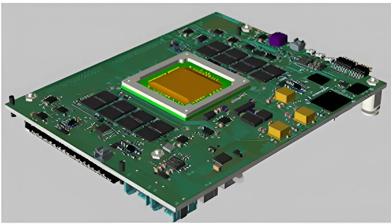
Som-zu48dr
-
Unique system-on-module approach enables deployment in
custom form factors
▪ Incorporates Xilinx RF-SoC FPGA XCZU48DR
▪ Onboard 4-32 GB of DDR4 SDRAM for PS and PL
▪ LVDS connections to the FPGA for custom I/O
▪ GT connections for gigabit serial communication
▪ Board Support Package (BSP) for software development
▪ FPGA carrier board (EVK) for development
| Title | Details |
|---|---|
| Field Programmable Gate Array |
Type: Xilinx RF-SoC FPGA XCZU28DRFSVG1517 |
| RF Input/Output |
Analog Inputs ▪ Quantity: 8 ▪ Connector: Board-to-board, single-ended ▪ Input Type: Single-ended A/D Converters ▪ Quantity: 8 ▪ Sampling Rate: 5 Gsps ▪ Input Range : 30 MHz to 6 GHz ▪ Resolution: 14 bits ▪ RF Input Bandwidth: 30MHz to 6 GHz Analog Outputs ▪ Quantity: 8 ▪ Connector: Board-to-board ▪ Input Type: Single-ended D/A Converters ▪ Quantity: 8 ▪ Sampling Rate: 10 Gsps ▪ Max Output Frequency : 10 GHz ▪ Resolution: 14 bits ▪ Output Range : 30 MHz to 6 GHz Sample Clock ▪ Source: SOM internal ▪ Mode: PLL clocking modes GPIO: FMC Vita 57.4 Compliant |
| Processor System |
Quad-core 64-bit ARM Cortex-A53 ▪ -2 Speed: Up to 1.2 GHz (-2 speed grade) |
| Programmable Logic I/O |
Programmable I/O’s: 75 pairs of LVDS connections /single-ended |
| Highspeed Processor I/O |
GT: 32 full-duplex lanes @ 36 Gb/sec GPIO: 16 differential/single-ended Additional Interfaces: I2C, SPI, SD/EMMC, UART, Ethernet |
| Memory |
Type: DDR4 SDRAM ▪ Quantity: Two banks ▪ PL 4 GB, upgradable to 32GB; 64-bit (FPGA) ▪ PS 4 GB, upgradable to 32GB; 64-bit (ARM) ▪ Boot Memory • Flash: 8 GB EMMC • Flash: 256 MB QSPI • NaND: SD 3.0 provision |
| SDFEC |
8 Nos of SDFEC for LDPC Support per SOM |
| Physical |
Dimensions: ▪ Length: 130.05 mm (5.12 in) ▪ Width: 104.04 mm (4.1 in) ▪ Height: 34.8 mm (1.37 in) Operating Temperature: 0 °C-70 °C |
| Title | Details |
|---|---|
| Synchronization |
Analog Inputs/Outputs ▪ RF Port Synchronization : Provision for RF phase and frequency Synchronization across multiple SOMs extending effective number of TX and RX RF ports to 16 ,32 ,64 etc. ▪ TX OP1dB : + 20 dBm ▪ RX IP1dB : -8 dBm ▪ RX Noise Figure : ≤10 dB @ 2.4 GHz ▪ Input Clock ref : PPS, 10MHz-700 MHz sync from PTP, GPS, Ext ref. Other Inputs/Outputs ▪ 100G QSFP Ethernet: 2 nos per carrier. Can be extended to 4,6,8 etc. due to modular construction to integrate multiple Carriers into a single integrated EVK ▪ 1G Ethernet : 1 nos per carrier. Can be extended across carriers ▪ PCIE x8 Connectors for synchronization across carriers: 2 per carrier. Can be extended across carriers ▪ SSD: Supports 1 sata link per carrier. Can be extended across carriers ▪ USB: 1 USB 3.0. Can be extended across carriers. ▪ Debug Interfaces: JTAG & UART via USB 2.0 Bridge ▪ Display Port: Display Port V1.2 TDP: 100W @ 12V DC input supply |
Sign up to get the latest updates
Stay updated on the latest trends.